PAGED memory on HCS08 / HCS12
AC96/AC128 in MultiProg works fine out of the box — read, write, verify and TRIM all "just work"; the programmer takes care of paged memory and the firmware format on its own. No manual PPAGE wrangling is needed for everyday use.
This article is educational, for those who want to understand how paged memory is wired up on HCS08, why USBDM and MultiProg dumps look different, and how to convert firmware between the two formats when that becomes necessary.
Probably every electronics engineer has had their brain melt while trying to figure out the memory map and the paged-memory mechanism (PAGEd memory) on the HCS08 / HCS12 MCU families (MCU = microcontroller).
These chips are old and their era is over, but we still bump into them from time to time. So we decided — partly to keep our own notes straight — to spell the whole thing out properly here.
We are all used to linear memory: at address 0x0000 lives one and only one byte, at 0x0001 the next, at 0x0002 the one after that, and so on until you run out. Like a regular book: page 5 always says what page 5 says, and to get there you just open the book at page 5. The address is the pointer to the byte, with nothing in between.
A linear memory layout is logical and sequential, which makes it easier to wrap your head around.
0. What is it, and why is it here?
10 years ago, when I first ran into the MC9S12C128, I thought paged memory was some kind of fancy feature only the chosen few really understood. As in: how it works is obvious, but why anyone would design it that way — that, only the super-developers knew.
After spending the last few months elbow-deep in this family, I can say with confidence: it's a kludge — a temporary, imperfect, workaround-style solution that mostly creates extra problems.
This article keeps coming back to Application Note AN3730 — the vendor itself spells it out in the very first sentence:
«Memory paging provides digital systems with greater memory addressing capabilities without expanding basic architecture resources, such as bus size or address pointers.» — AN3730 §1, opening paragraph.
Translation: "so we wouldn't have to widen the bus or grow the pointer — i.e. not touch the architecture — but still ship an MCU with more memory, we came up with this clever trick". The decision was driven purely by what was convenient for the vendor.
1. So what's the gist?
The gist is the dual coordinate system. Pages (PAGE) have no real address; you can reach them only through a special mechanism. One coordinate system is ordinary and linear — that's where RAM, the registers, and some of the pages (in chunks) live. The other one is where the pages exist, but they aren't actually in the main memory map — only fragments of them peek through the PPAGE window.
Because of this, every programmer-software vendor can decide on their own how to assign addresses, splits and so on to these regions. Hence the firmware-file mess — there's no single standard in practice.
If you have ever read an MC9S08AC128 with two different programmers, you've noticed: the dump files look completely different. Same chip, same content, but the addresses in the file are different.
This is where the dual coordinate system starts playing tricks on you. Watch closely: in the linear space, a 7952-byte chunk of page 0 sits at 0x20F0 onwards.
This is Figure 4-1 from the MC9S08AC128 Reference Manual. Half the engineers who see it for the first time conclude that page 0 starts at 0x20F0. The catch is that page 0 exists separately and has its honest 16 KB — like every other page. A 7952-byte tail of it just "sticks out" in the linear space (presumably a manufacturing quirk).
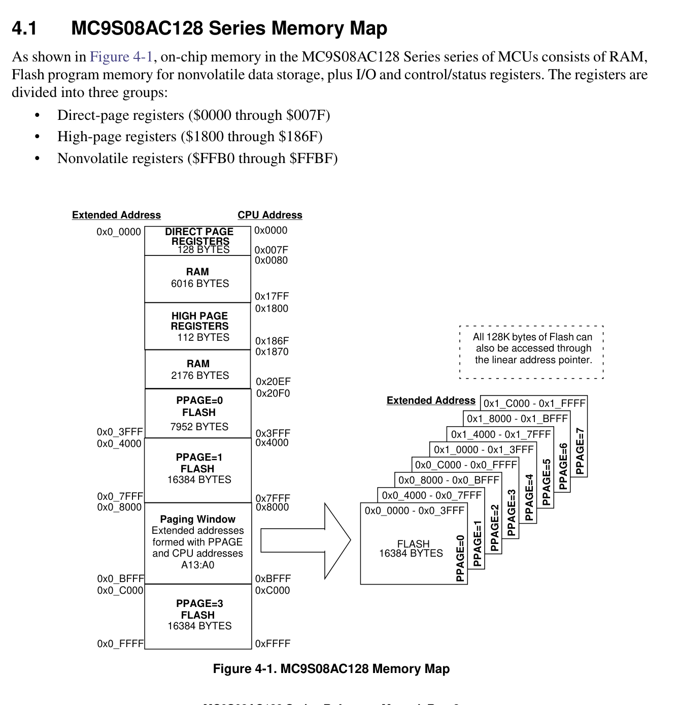
The closest everyday analogy is a housing development. Three families (16 KB each) live in their own houses, with proper street numbers and individual entrances — that's the linear memory. The remaining five families (also 16 KB each) the developer crammed into a single apartment building reached by one road and a couple of side paths. On paper there are 8 families — everything looks great.
The smaller variants (anything up to ~64 KB of flash) fit inside the 16-bit core pointer (addresses up to 0xFFFF) and behave as ordinary linear memory. The larger ones — the parts with 96 or 128 KB of flash: AC96/AC128, QE128, DZ128 and friends — overflow what the pointer can cover, but the memory is still there. This is exactly where paged memory steps in and closes the addressing gap for the vendor.
Result: you can't just walk through it sequentially. In ordinary linear memory you can read byte 1, 2, 3, … in one continuous sweep, like turning the pages of a book. With the larger, paged variants that won't fly — you first have to set the window to expose a specific page.
A modern microcontroller (a 32-bit Cortex-M0+ with 128 KB of flash) has none of these problems — you address byte 47,000 as "byte 47,000", end of story. Paged access today survives mostly in EEPROM chips; you won't run into this kind of design in any modern MCU.
2. How it's organised
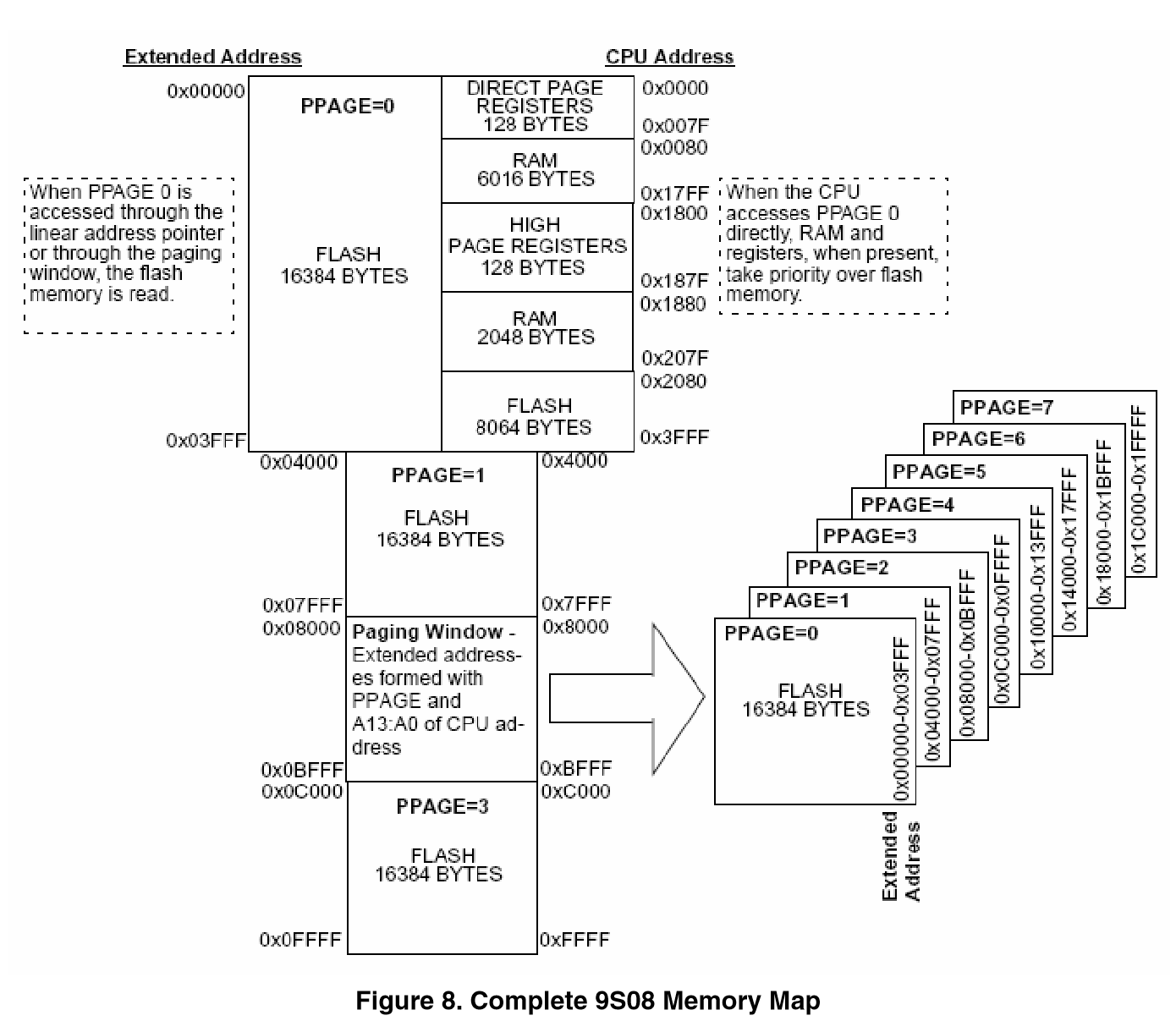
What we can see on this picture:
0x8000–0xBFFFis the PPAGE window (remember the "one road" analogy?). AfterPPAGE = N, the CPU sees the physical pageN(16 KB) in this window.- The fixed windows
0x4000–0x7FFF(page 1) and0xC000–0xFFFF(page 3) are combined: pages 1 and 3 hang in both coordinate systems at the same time — they are visible both directly through their fixed windows and through the PPAGE window (whenPPAGE = 1andPPAGE = 3respectively). So everything that traditionally lives at the top — the reset vector0xFFFE/F, the security byteNVOPT@0xFFBF, the trim byte0xFFBE— physically belongs to page 3, yet the CPU sees those bytes "directly" as if they were ordinary linear memory. All in all, about 2.5 pages stick out in the direct CPU view on AC96/AC128: the page 0 tail (0x20F0–0x3FFF, the lower 8432 bytes are shadowed by RAM and registers), all of page 1, and all of page 3. The rest is reachable only through the PPAGE window.
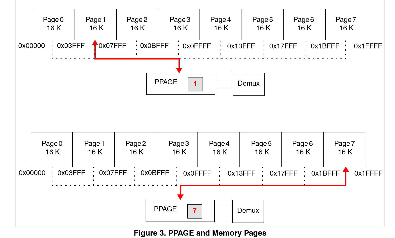
The PPAGE register is the "page selector": write a number into it, and that page becomes visible in the PPAGE window. Change the number — see a different page. In the figure above: PPAGE = 1 → the CPU sees page 1, PPAGE = 7 → the CPU sees page 7.
PPAGE on AC96/AC128 is a 3-bit field (values 0..7), so the maximum addressable flash is 8 × 16 KB = 128 KB. AC96 is just shorter: pages 0..5 = 96 KB.
3. On firmware compatibility
The MCU is one thing; the file you save on the host — given all this unique technology — is a separate headache. There are two competing layout formats for laying paged flash into an S-record, and both are in active use.
"S19 with PPAGE in the high byte" — USBDM Memory Dump
When USBDM Memory Dump saves paged memory, it generates 24-bit addresses: the high byte is PPAGE, the low 16 bits are the CPU view inside the PPAGE window:
address_in_file = (PPAGE << 16) | cpu_addr // cpu_addr in 0x8000..0xBFFF
Page N ends up in the file at addresses 0xN8000..0xNBFFF. The original USBDM uses the same format when dumping an MC9S08AC128 — the output is an S19 in which 8 page-slots of 64 KB each are spread across addresses 0x08000..0x7BFFF (≈ 475 KB of occupied range out of ≈ 512 KB potential), even though the file holds only 128 KB of real data. In each slot, only the top 16 KB (0xN8000..0xNBFFF) carry data; the other 48 KB are empty: the lower 32 KB (0xN0000..0xN7FFF) and the upper 16 KB (0xNC000..0xNFFFF, which would have overlapped with the fixed window 0xC000..0xFFFF).
"Flat linear" — MultiProg
We use a different format: lay the pages down densely, one after another, starting at 0x8000, with no gaps:
address_in_file = 0x8000 + (PPAGE * 0x4000) + (cpu_addr - 0x8000)
An AC128 dump in this format is exactly 128 KB of contiguous data from 0x8000 to 0x27FFF in physical-page order. MultiProg uses precisely this format so that firmware files match byte-for-byte with Orange 5: write a dump in one program, read it in the other, and you get the same bytes at the same offsets.
Address comparison
The same MC9S08AC128, read with two different programs, produces:
| Page | Original USBDM (PPAGE in high byte) | MultiProg (flat) |
|---|---|---|
| 0 | 0x08000 – 0x0BFFF | 0x08000 – 0x0BFFF |
| 1 | 0x18000 – 0x1BFFF | 0x0C000 – 0x0FFFF |
| 2 | 0x28000 – 0x2BFFF | 0x10000 – 0x13FFF |
| 3 | 0x38000 – 0x3BFFF | 0x14000 – 0x17FFF |
| 4 | 0x48000 – 0x4BFFF | 0x18000 – 0x1BFFF |
| 5 | 0x58000 – 0x5BFFF | 0x1C000 – 0x1FFFF |
| 6 | 0x68000 – 0x6BFFF | 0x20000 – 0x23FFF |
| 7 | 0x78000 – 0x7BFFF | 0x24000 – 0x27FFF |
| File address span | ≈ 512 KB (48 KB gaps between data blocks) | 128 KB (dense) |
The files are not byte-identical until you convert one into the other, but they describe exactly the same bytes on the physical die. Converting an address from the USBDM format (with PPAGE in the high byte) into the flat one:
linear = 0x8000 + ((usbdm >> 16) * 0x4000) + (usbdm & 0x3FFF)
…and back:
usbdm = (((linear - 0x8000) / 0x4000) << 16) | 0x8000 | ((linear - 0x8000) % 0x4000)
4. FAQ
Q. Are MultiProg and USBDM S19 files directly interchangeable in both directions?
No. Our flash region is declared with start_addr = 0x8000 and a contiguous size — the loader knows nothing about the gaps in the USBDM layout. The reverse is also true: USBDM/CodeWarrior expect addresses with PPAGE in the high byte, while MultiProg outputs a flat range. In either direction the file has to be converted first — either with the Lua script below or with any hex editor and a couple of lines of scripting.
Q. Is there a ready-made script that converts into MultiProg format? Here is an example Lua script that turns a dump in USBDM format (PPAGE in the high byte — the left column of the address comparison) into the flat MultiProg format (the right column). The Lua engine is built into MultiProg — see the API reference.
-- USBDM S19/HEX (PPAGE in the high byte) → flat S19 for MultiProg
-- Parse the input by hand via mp.file.read_text — without mp.file.load,
-- so we don't touch the active target's buffer and don't hit "read-only".

local in_path  = mp.ui.open_file_dialog("USBDM dump (PPAGE in high byte)", nil, "S-Record (*.s19 *.hex)")
if in_path == "" then return end
local out_path = mp.ui.save_file_dialog("Flat S19 for MultiProg", nil, "S-Record (*.s19)")
if out_path == "" then return end

local text, err = mp.file.read_text(in_path)
if err and err ~= "" then mp.log.error(err); return end

local out = {}
for line in text:gmatch("[^\r\n]+") do
    if line:sub(1, 1) == "S" then
        local t = line:sub(2, 2)
        if t == "1" or t == "2" or t == "3" then
            local count       = tonumber(line:sub(3, 4), 16)
            local addr_chars  = (t == "1") and 4 or ((t == "2") and 6 or 8)
            local addr        = tonumber(line:sub(5, 4 + addr_chars), 16)
            local data_start  = 5 + addr_chars
            local data_chars  = (count - addr_chars // 2 - 1) * 2
            local data_hex    = line:sub(data_start, data_start + data_chars - 1)
            local data        = mp.utils.hex_to_bytes(data_hex)

            local ppage = (addr >> 16) & 0xFF
            local cpu   = addr & 0xFFFF
            local linear
            if cpu >= 0x8000 and cpu <= 0xBFFF then
                -- PPAGE window: PPAGE * 16 KB + offset inside the window
                linear = 0x8000 + ppage * 0x4000 + (cpu - 0x8000)
            elseif cpu >= 0xC000 and cpu <= 0xFFFF then
                -- fixed window — always page 3
                linear = 0x8000 + 3 * 0x4000 + (cpu - 0xC000)
            else
                mp.log.warn(string.format("skip @ 0x%05X (out of paged range)", addr))
                goto continue
            end
            table.insert(out, { address = linear, data = data, size = #data })
            ::continue::
        end
    end
end

local ok, e = mp.file.save(out_path, out)
if ok then
    mp.log.success(string.format("saved %s (%d blocks)", out_path, #out))
else
    mp.log.error(e)
end
This script isn't bundled with MultiProg's built-in examples yet — we'll add it in one of the upcoming releases. For now, just paste the code above into the Script Console.
The reverse conversion (flat → USBDM) is written symmetrically — the formula is in the tip block in §3.
Q. After erase, verify complains about bytes 0xFFBD, 0xFFBE and 0xFFBF. Is that a bug?
No — that's the quirk of these three "live" bytes. All of them physically live in page 3 and are visible through the fixed window 0xC000–0xFFFF. Their addresses in the MultiProg UI (the same for AC96 and AC128):
| Byte | CPU address | In the MultiProg buffer |
|---|---|---|
| NVPROT | 0xFFBD | 0x17FBD |
| ICGTRM | 0xFFBE | 0x17FBE |
| NVOPT | 0xFFBF | 0x17FBF |
0xFFBE— ICGTRM (internal-oscillator trim). A per-die factory calibration: on the test bench, the vendor picked the value at which the internal RC oscillator produces the right frequency. After a full erase this byte becomes0xFF, and the oscillator drifts off — code running on it may end up at the wrong frequency or fail to start at all. For exactly this case MultiProg has a TRIM dialog with Test Calibration that lets you pick a fresh trim value for the specific MCU at hand.0xFFBF— NVOPT (non-volatile option byte). After a proper erase this byte must be0xFE(SEC[1:0] = 10— security off), the "open" state in which the MCU is still reachable over BDM. The value0xFF(which a naïve "all-bits-to-1" erase would leave behind) corresponds toSEC[1:0] = 11→ MCU in secured mode, and a BDM session can no longer be opened. Decent programmers (MultiProg among them) use the Mass Erase Unsecure command — it wipes the flash and leaves NVOPT in the required0xFEin the same step, so the MCU doesn't lock itself away from the user.0xFFBD— NVPROT (non-volatile flash protection). After erase it's0xFF, and that's normal —0xFFmeans "flash write-protection off", the MCU stays programmable. Verify will only flag this byte if the source dump had something other than0xFFhere.
Q. Where can I look this up in the documentation?
MC9S08AC128 Reference Manual Rev. 3 — §4.1 (paged memory model), §4.4 (flash command sequence), Table 4-2 sheet 3 (the direct-page register list, including PPAGE@$0078).
AN3730 — Understanding Memory Paging in 9S08 Devices — a paper that does a great job describing the entire paged-memory mechanism; the figures above are taken from it.
Bottom line
That's it — we've walked through how paged memory is wired up on AC96/AC128, what makes USBDM and MultiProg dumps look different, how to convert between them, and why NVOPT = 0xFE after erase is the MCU's correct "unsecured" state rather than a bug.